Research
Research Area II: On-Chip Lasers & Integration - Photonic Microsystems Group
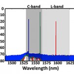
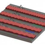
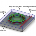
1.8.2015The ability to reliably fabricate silicon microphotonic devices and systems in a CMOS-compatible process is the key to the success of silicon photonics. Our group established a collaboration with the College of Nanoscale Science and Engineering (CNSE) at the University of Albany. Together we developed the first 300mm silicon photonics process ever demonstrated. The process flow itself consists of two etch steps in the silicon layer, four implants, two dual damascene copper interconnect and via layers, three layers of silicon nitride, germanium, etched facets for low-loss coupling, and a trench etch for the incorporation of an active erbium doped layer for on-chip lasers and optical amplifiers. Using this recently developed process flow, our group has demonstrated erbium-doped lasers in a manner that allows for direct integration of lasers on-chip (left figure). Already, distributed feedback (DFB) and distributed Bragg reflector (DBR) lasers have been demonstrated on-chip across a broad range of wavelengths and with output powers as high as 75mW and in passive demonstrations, channel alignment to within 10-picometers has been achieved (middle figure). Besides, microdisk cavity laser (right figure) has also been demonstrated as a compact (~80um radius) on-chip laser source. To achieve future advances, rigorous electromagnetic design must be coupled to CMOS circuitry to drive, minitor, and control the performance of the microphotonic circuits and networks. The approach used in our group utilize wafer-sacle 3D integration with through oxide vias that enable the high-densities and low parasitics offered by direct integration while maintaining the flexibility to separately optimize the photonics and CMOS processes common to hybrid integration techniques.


